Photomasks for Various Applications
About Photomasks for Various
Applications
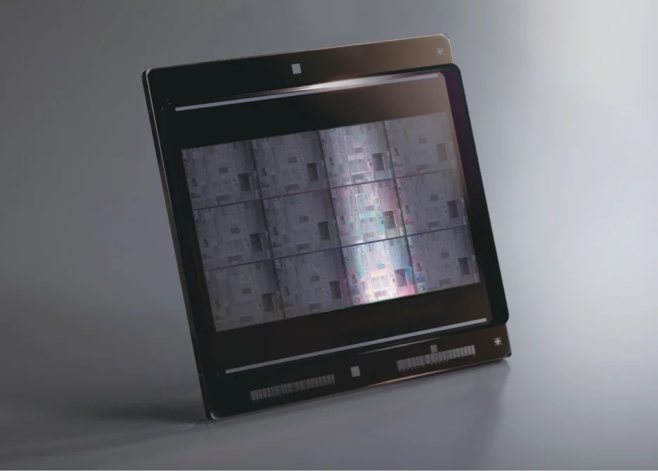
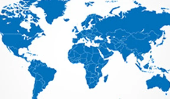
Toppan Photomask is providing high resolution, highly reliable photomasks not only for semiconductors, but also for different industrial areas / research purposes, utilizing its microfabrication technology.
feature-5
Features
Use of the Photomasks
Toppan provides photomasks to various markets including industry, R&D, etc.
<Instances of Supply>
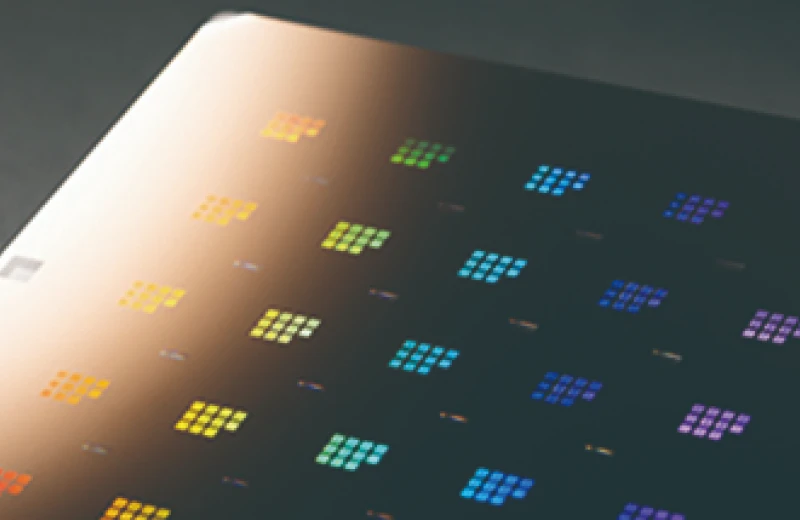
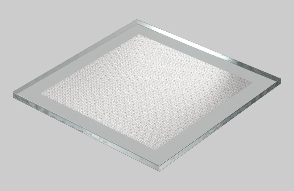
Masks for MEMS
Mask for IC bump packaging
Masks for Semiconductor Packaging Substrates
Masks for LED Masks for Thermal Head
Mask for Device Accuracy control
Test Chart
Master masks for High-resolution Printing
Masks for various R&D etc.
Please make inquiries for more information.
Specification Outline
■ Mask Size 5inch x 5inch (127.0 mm x 127.0 mm) , 6inch x 6inch (152.4 mm x 152.4 mm)
Please contact us about other sizes.
■Acceptable Data Format GDS, GBR, or Design diagram
■Substrate, etc. Synthetic Quarts, Soda-lime Glass / Thickness: 0.09~0.25 inch (t)
Pellicle mounting possible

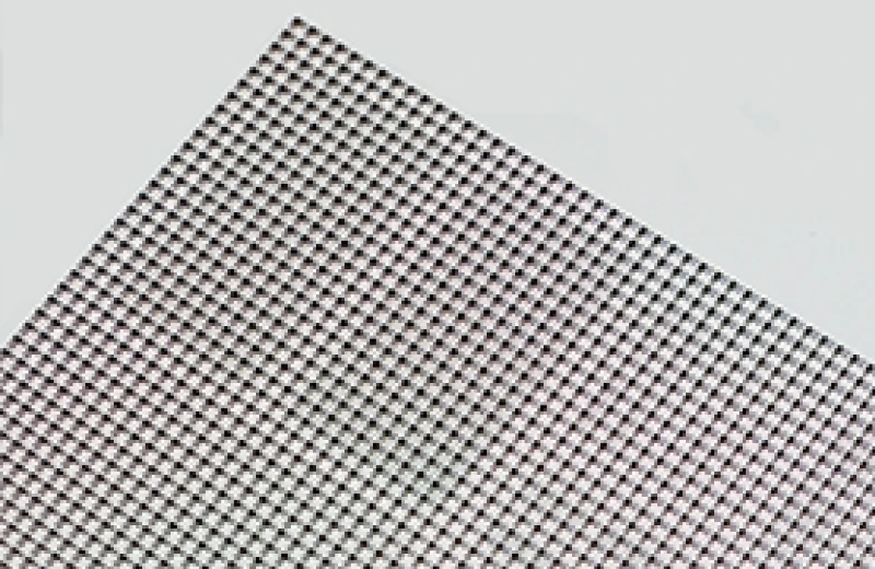
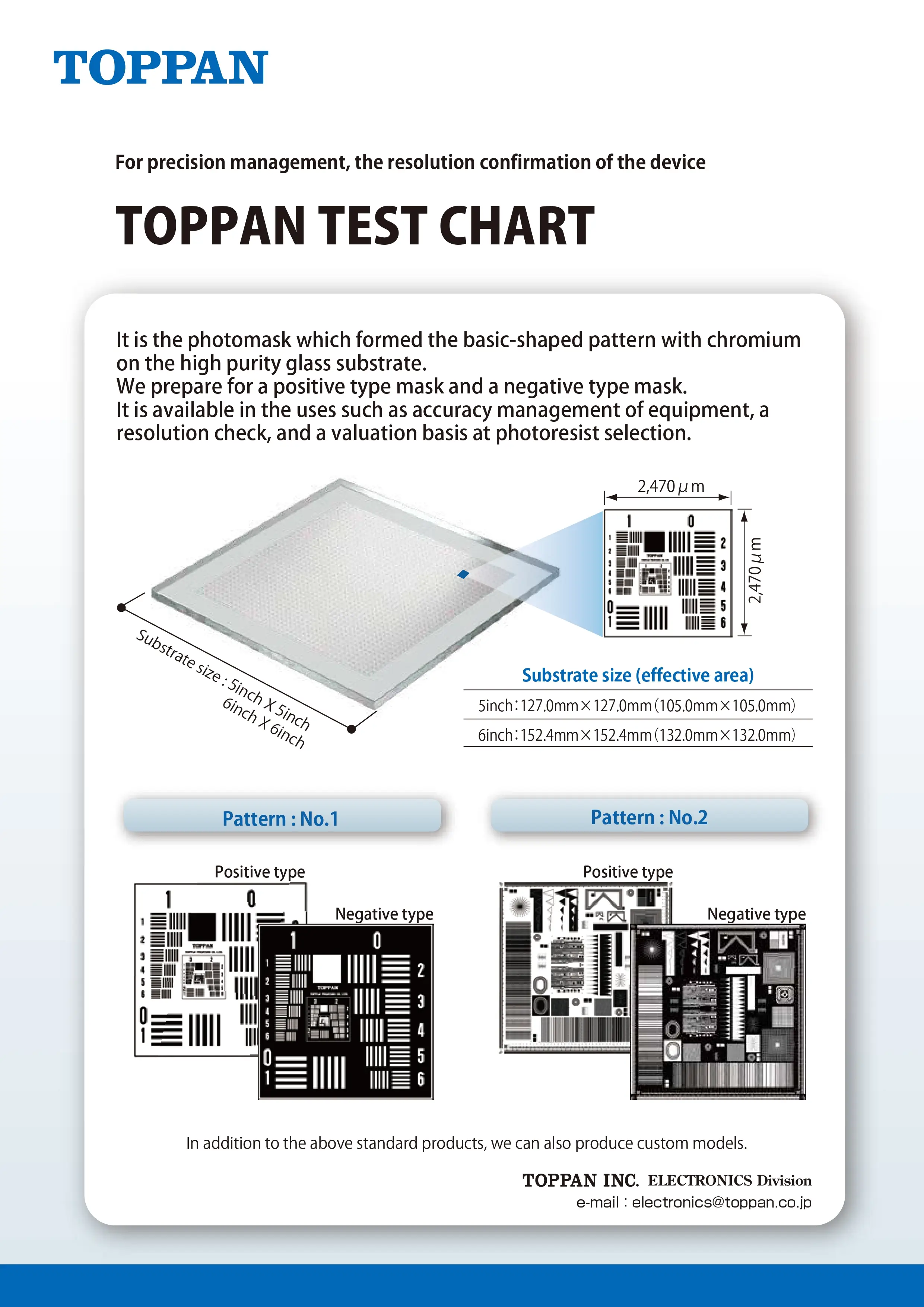
Toppan Test Chart
Toppan Test Chart is the photomask which formed the basic-shaped pattern with chromium on the high purity glass substrate.
We prepare for a positive type mask and a negative type mask.
It is available in the uses such as accuracy management of equipment, a resolution check, and a valuation basis at photoresist selection.

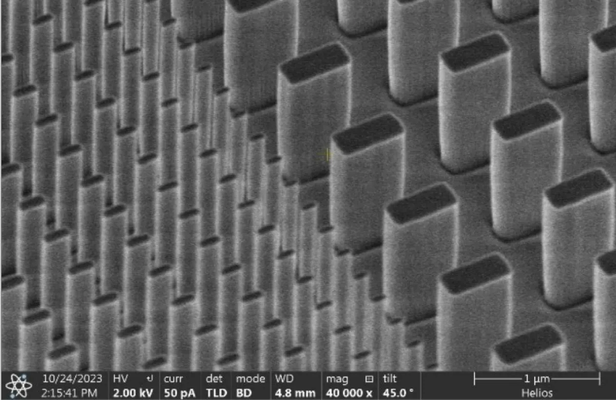
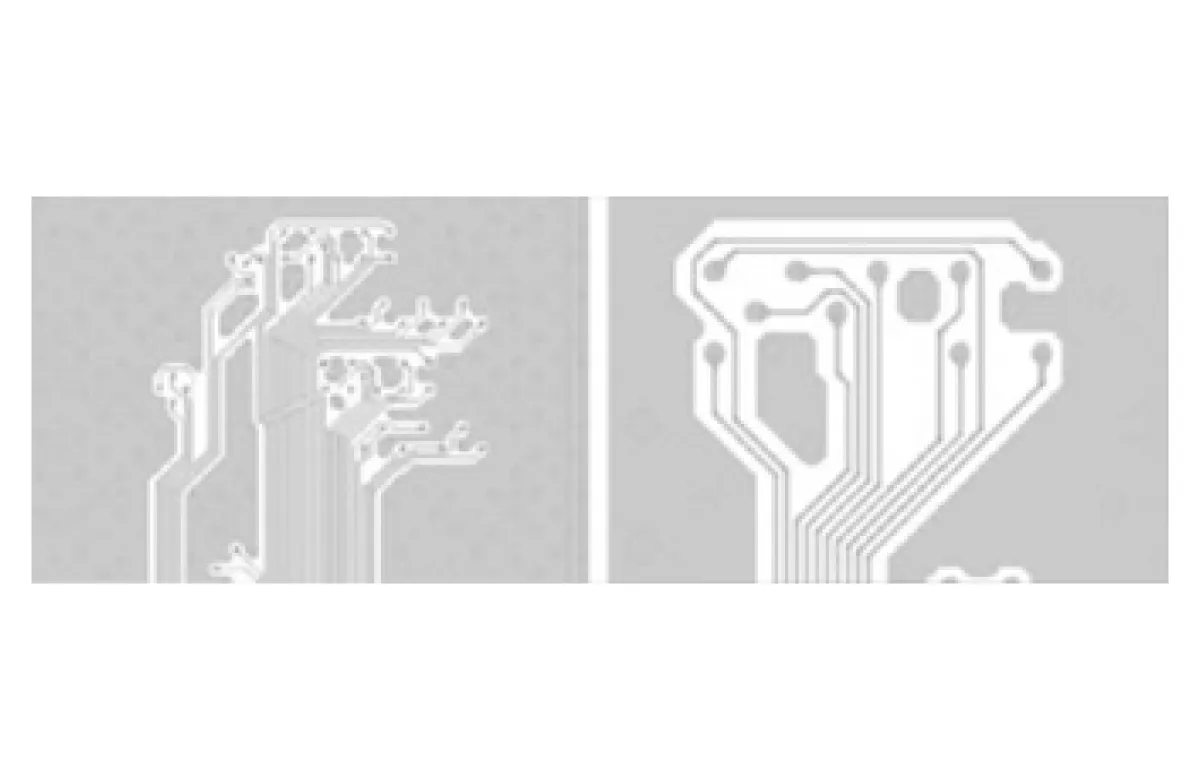
3D Photomasks
3D Mask (gray-scale mask, gray-tone mask) is a 3D photomask, applying the well-established photomask technology including high resolution. 3D structures including micro lens are formed by controlling transmission volume of the light.
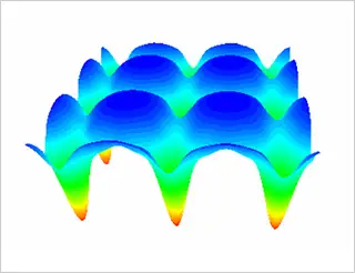
Microlens Structure (Prolith)
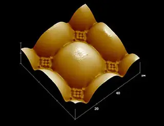
Transferred Image of 3D mask (AFM image of resist profile)

Examples of pattern type
feature-5
Download Brochure
feature-5