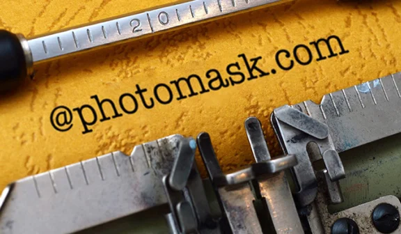
Photomasks for Semiconductors
About Photomasks for
Semiconductors
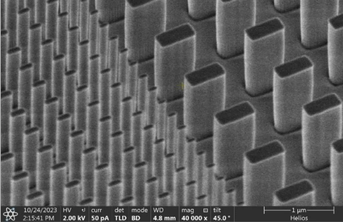
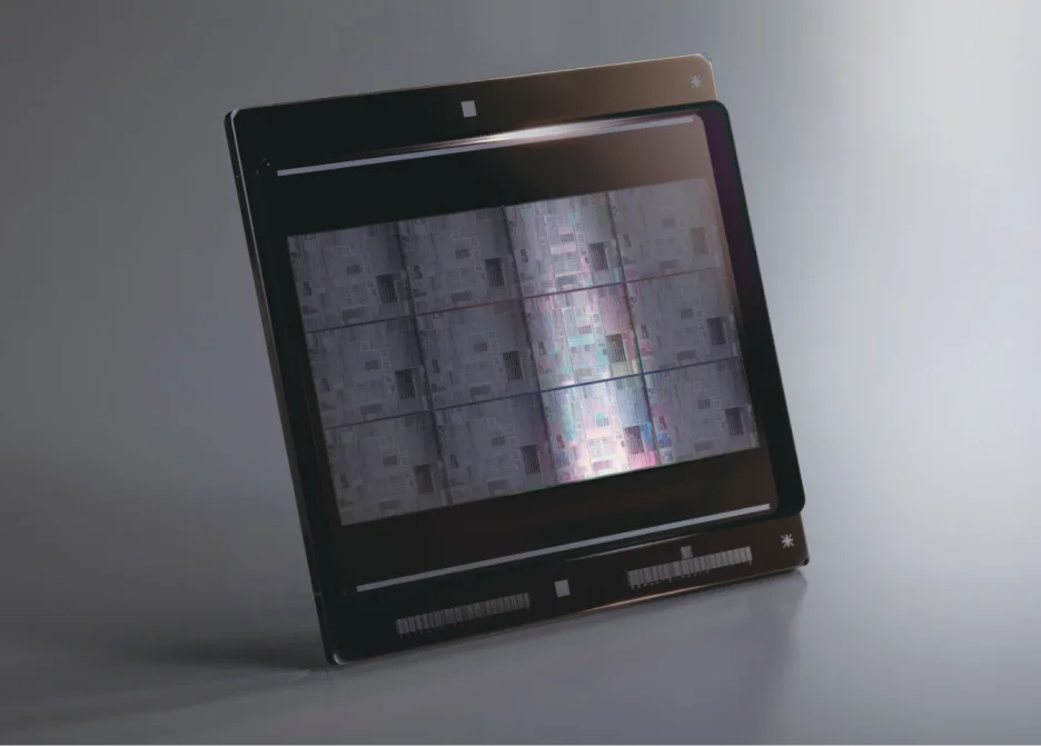
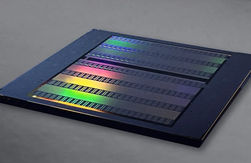
Photomasks play an important role in the semiconductor manufacturing process and are the master plates used to transfer circuits onto semiconductor wafers. Based on circuit data, an electron beam is used to create an electronic circuit pattern on a photomask substrate (mask blank), which is then etched with chemicals, stripped of photoresist (photosensitive material), cleaned, measured, and inspected before the photomask is completed.
feature-5
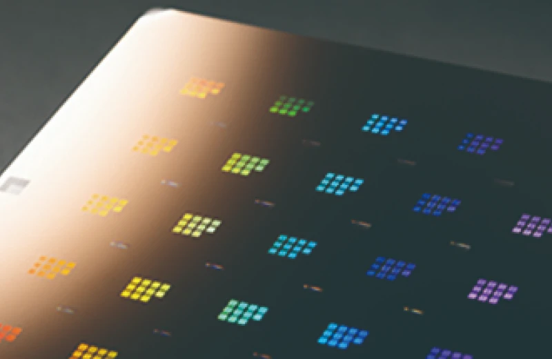
Semiconductor Photomask Lineups
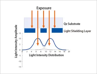
Binary Masks
Structure of binary mask is simple; it is a photomask blank covered with patterned layer of opaque material. Its transmission characteristics are either transparent or non-transparent. Binary mask is used for building a pattern in which line width being larger than the exposure wave length.
the halftone phase shift mask used for immersion lithography for 32nm half-pitch or beyond.
Toppan and its blanks vendor have co-developed new type of binary blanks with superior workability (OMOG: Opaque MoSi on Glass). They have managed to create blanks for binary masks with better CD performance and higher resolution.
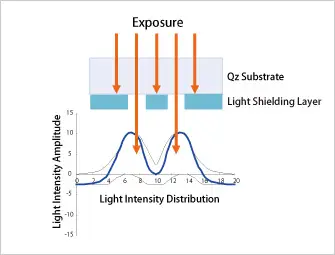
Phase Shift Masks
Phase-shifting mask (PSM) has achieved improved wafer printability with higher resolution and increased DOF (Depth of Focus), by controlling the phase shift and the transmission rate. This is a standard technology for lithography in which line width being smaller than the exposure wave length.
Most well known PSM is Halftone mask (Attenuated PSM) and Levenson mask (Alternating PSM).
EUV Photomasks
EUV is a number one candidate of next generation lithography technique. EUV lithography uses EUV light (13.45nm), shorter wave length than existing DUV (ArF: 193nm), in which enabling us to fabricate smaller patterns. Unlike conventional DUV, EUV lithography requires reflective optics for wafer exposure systems and for masks, as EUV technology cannot focus light via conventional lens optics.
feature-5